Research
Controlling the Orientation, Edge Geometry and Thickness of Chemical Vapor Depostion Graphene ACS Nano 24 Jan 2013 DOI: 10.1021/nn3049297
A new way of growing graphene without the defects that weaken it and prevent electrons from flowing freely within it could open the way to large-scale manufacturing of graphene-based devices with applications in fields such as electronics, energy, and healthcare.
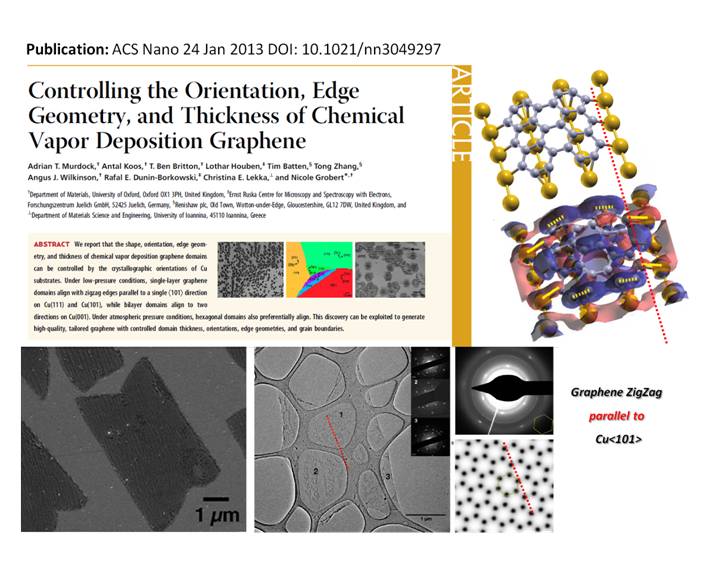
A team led by Nicole Grobert has overcome a key problem of growing graphene by chemical vapour deposition. by using copper substrate to control the orientation of growing graphene flakes. Where these flakes, called ‘domains’, are well-aligned, which will create a neater, stronger, and more ‘electron-friendly’ material.
The Oxford-led team, which includes researchers from Forschungszentrum Juelich Germany, the University of Ioannina Greece, and Renishaw plc, has also shown that it is also possible using the new technique to selectively grow bilayer domains of graphene – a double layer of closely packed carbon atoms – which are of particular interest for their unusual electrical properties.
http://www.materials.ox.ac.uk/blog/148/544/Controlling-the-Orientation-Edge-Geometry-and-Thickness-of-Chemical-Vapor-Depostion-Graphene.html
The UoI contribution:
The orientation of the graphene flakes along e.g. the Cu(110) surface <101> direction were supported by Density Functional Theory calculations revealing that the zig-zag edge is preferentially aligned along the surface channel due to Cu3d- C2p hybridizations, thus reducing the lattice mismatch.